
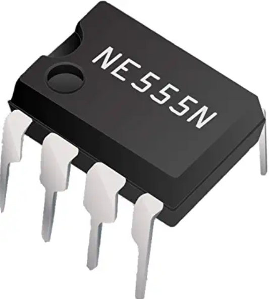
IC or Integrated Circuit is an electronic component made using fundamental electronic components like resistors, inductors, capacitors, transistors, etc fabricated on a small semiconductor chip. There are ICs for almost every possible application of electronics. We have ICs for flip-flops, amplifiers, counters, memory, microprocessor, microcontroller, etc. In this article, we are going to discuss one of the most popular and widely used ICs – 555 IC.
555 IC is an 8 pin IC used for generation of oscillation and time delays. This IC comes in different packages like PDIP, SOIC, VSSOP, etc. These packages mainly differ in sizes. It usually operates from 4.5 to 16 volts. 555 IC is mainly used in the generation of clock pulses, time delays, and in the application of Pulse Width Modulation (PWM), Pulse Position Modulation (PPM), etc. In this article, we are going to describe the architecture and pin-out diagram of the IC and a simple application of 555 IC as a clock pulse generator in astable mode.
The architecture of 555 IC
The circuit of 555 IC consists of a voltage divider, two comparators, an SR flip-flop, an output unit, and a ‘discharge’ transistor. Let’s discuss them one by one.
- Voltage Divider: The voltage divider is made using three 5KOhm resistors connected in series. From these three resistors, this IC has gotten its name. From the VCC pin, the voltage at the internal nodes of this series is 2/3 and 1/3 of VCC respectively.
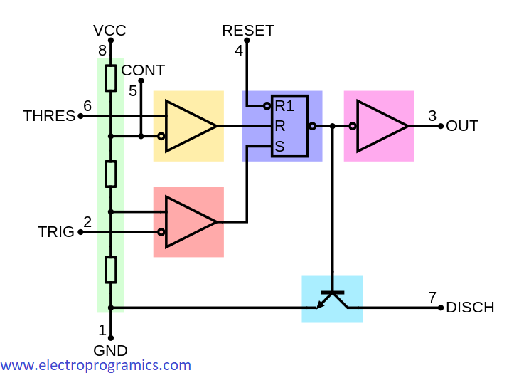
- Comparators: we have two comparators. In the case of the top one (as shown in the diagram) the negative terminal is connected to the node whose voltage is 2/3 of VCC. And the positive terminal of the comparator is connected to the threshold pin. When the output of the threshold pin is greater than 2/3 of VCC, the output of that comparator becomes high. The output of this comparator is connected to the reset or R pin of the flip-flop. The negative terminal of this comparator is also connected with the Control pin which controls the pulse width of the output waveform.
Now, in the case of the second comparator, the positive terminal is connected to the node whose voltage is 1/3 of VCC, and the negative terminal is connected to the trigger pin. When the voltage at the trigger pin falls below 1/3 of VCC, the output of the comparator becomes high. The output of this comparator is connected with the set pin or the S pin of the flip-flop.
- Flip-flop: We have an SR flip-flop. The Spin and the R pin are connected to the output of the comparators. The reset pin of the flip-flop is connected to the reset pin of the 555 IC. The truth table of the SR flip-flop is given here. Taking the input from the comparators and following the truth table, the flip-flop gives it output which is the input of the output unit.
- Output Unit: This unit, after taking input from the flip-flop, produces the output of the IC.
- Discharge Transistor: We also have a discharge transistor connected with the output of the flip-flop. To control the output waveform, we have to connect some resistors, capacitors externally. This transistor is used to discharge capacitors connected with the trigger or threshold pin.
Pin-Out Diagram
555 IC has a notch at one side of the top of the IC using which we can identify the number of the pins. The pin diagram of 555 IC is given below with the description of the pins.
- Pin 1 – GND: It is an output pin that is connected to the ground terminal of the voltage supply.
- Pin 2 – Trigger: This is an input pin that triggers the output of SR flip-flop to change its state from set to reset and vice versa.
- Pin 3 – Output: Pin 3 is the output pin. We get the output waveform through this pin.
- Pin 4 – Reset: It is an input pin. When it is connected to the ground, it turns the output to zero or resets the output. This is why usually this pin is connected to the VCC.
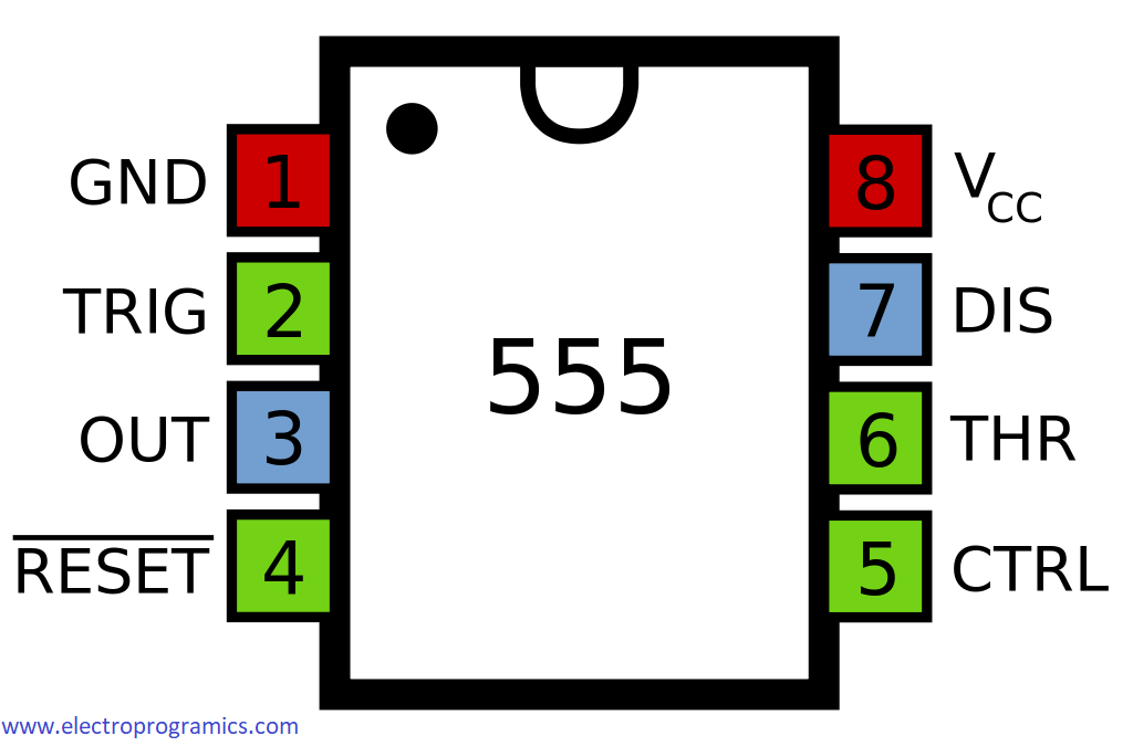
- Pin 5 – Control: It is an input pin used to determine the pulse width of the output.
- Pin 6 – Threshold: This is an input pin that is also responsible for changing the output of the SR flip-flop.
- Pin 7 – Discharge: This pin is used to discharge the external capacitors connected to the trigger pin or threshold pin of the IC.
- Pin 8 – VCC: This pin is connected to the positive terminal of the voltage supply.
Generation of Clock Pulse in Astable Mode
A clock pulse is an electronic signal used to synchronize an electronic circuit. It is usually a square wave which means its amplitude has only two values – high and low. We can generate a clock pulse using 555 IC in astable mode using the circuit diagram given here. The period of output waveform depends on the charging and discharging period of the capacitor C and the value of R1 and R2. By changing the value of R1, R2 and C we can change the time period, time high, time low, duty cycle, etc of the output waveform.
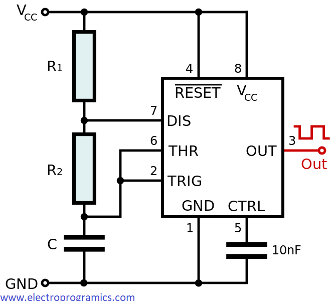
The image of the output waveform of the above circuit is given below. We have considered only three parameters which are Time Period (T), Time High (TH), Time Low (TL). The value of these parameters can be calculated using the following formulas:
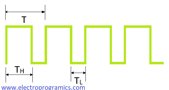
Firstly, T = 0.693 × (R1+2R2) × C second
and TH = 0.693 × (R1+R2) × C second
TL = 0.693 × R2 × C second
We have taken the unit of the resistors as Ohm and the unit of the capacitor as Farad. Using these parameters, we can calculate the other parameters of the waveform like duty cycle. If you need a clock pulse with specific parameter values, you can calculate the value of resistors and capacitors using these formulas. We can also make a led blink using this circuit by connecting the led between the output pin and ground.
Hope that you are clear with the topic NE 555 IC. If you have any doubts about the topic please feel free to comment below and you will be clarified.